bloc 33rd Square Business Tools - superconductivity 33rd Square Business Tools: superconductivity - All Post
Showing posts with label superconductivity. Show all posts

Tuesday, December 9, 2014

Superconductivity Understandings May Lead To Breakthroughs


 Superconductivity
Researchers have found that an infrared laser pulse briefly modifies the structure of a high-temperature superconductor and removes its electrical resistance even at room temperature.


I
n the 1980s, physicists first discovered a new class of materials based on ceramics. These materials conduct electricity at temperatures of around minus 200 degrees Celsius without losses, and were therefore called high-temperature superconductors. The compound yttrium barium copper oxide (YBCO) is one of these high-temperature superconductors and is one of the most promising materials for technical applications of the material, such as superconducting cables, motors and generators.

YBCOs crystal have a special structure: thin double layers of copper oxide alternate with thicker intermediate layers which contain barium as well as copper and oxygen. The superconductivity has its origins in the thin double layers of copper dioxide. This is where electrons can join up to form so-called Cooper pairs.

Cooper pairs can “tunnel” between the different layers, meaning they can pass through these layers like ghosts can pass through walls,in a type of quantum effect. The crystal only becomes superconducting however below a "critical temperature."

Above the critical temperature, this coupling between the double layers is missing, and the material becomes a poorly conducting metal.

Related articles
Andrea Cavalleri at the Max Planck Institute first discovered that when YBCO is irradiated with infrared laser pulses it briefly becomes superconducting at room temperature in 2013. The laser light had apparently modified the coupling between the double layers in the crystal.

The precise mechanism was unclear until the physicists were able to solve the mystery with an experiment at the Linac Coherent Light Source (LCLS) laser in the US, the world’s most powerful X-ray laser.

"It could assist materials scientists to develop new superconductors with higher critical temperatures and ultimately to reach the dream of a superconductor that operates at room temperature and needs no cooling at all."


“We started by again sending an infrared pulse into the crystal, and this excited certain atoms to oscillate,” explains Max Planck physicist Roman Mankowsky, lead author of the current study published in Nature. “A short time later, we followed it with a short X-ray pulse in order to measure the precise crystal structure of the excited crystal.”

According to the researchers, the infrared pulse had not only excited the atoms to oscillate, but had also shifted their position in the crystal as well. This briefly made the copper dioxide double layers thicker - by two picometres, or one hundredth of an atomic diameter - and the layer between them became thinner by the same amount. This in turn increased the quantum coupling between the double layers to such an extent that the crystal became superconducting at room temperature for a few picoseconds.

On the one hand, the new result helps to refine the still incomplete theory of high-temperature superconductors. “On the other, it could assist materials scientists to develop new superconductors with higher critical temperatures,” says Mankowsky. “And ultimately to reach the dream of a superconductor that operates at room temperature and needs no cooling at all.”

Until now, superconducting magnets, motors and cables required cooling to temperatures far below zero with liquid nitrogen or helium. If this complex cooling were no longer necessary, it would mean a breakthrough for this technology. This research may point to promising directions for understanding and development of higher temperature superconductors.


SOURCE  Max Planck Institute

By 33rd SquareEmbed

Thursday, April 10, 2014


 Superconductors
An international team of scientists has reported the first experimental observation of the quantum critical point in the extensively studied 'unconventional superconductor' TiSe2, finding that it does not reside as predicted within the superconducting dome of the phase diagram, but rather at a full GPa higher in pressure.


An international team of scientists has reported the first experimental observation of the quantum critical point (QCP) in the extensively studied “unconventional superconductor” TiSe2, finding that it does not reside as predicted within the superconducting dome of the phase diagram, but rather at a full GPa higher in pressure.

In the image above, an artist's conception of charge density wave domain walls in TiSe2 and the emergence of superconductivity through their quantum fluctuations.

The discovery of a new phase boundary has implications for our understanding of superconducting behavior.


The surprising result, reported in Nature Physics, suggests that the emergence of superconductivity in TiSe2 isn’t associated with the melting of a charge density wave (CDW), as prevailing theory holds; in fact the CDW’s amplitude decreases under increasing pressure, but does not disappear at zero resistance.

TiSE2 Crystals
TiSE2 Crystals used in the experiment
The researchers find that the emergence of superconductivity in this material is connected rather with the formation of domain walls between commensurate and incommensurate phase transitions. The discovery of this new phase boundary has implications for our understanding of superconducting behavior.

Related articles
The experiments, conducted by Young Il Joe, a graduate student working with condensed matter physicist Peter Abbamonte, employed a novel X-ray scattering technique at the Cornell High Energy Synchrotron Source (CHESS) to obtain the first ever measurements of the degree of commensurability of the CDW order parameter.

The researchers took advantage of the harmonics of the diffractive optics—usually filtered out in X-ray experiments—to take two readings simultaneously. The wavelengths of two simultaneous photon beams were carefully calibrated, one to measure the periodicity of the crystal lattice, the other to measure the periodicity of the electrons, and compare the two. At low energies, the CDW was found to be commensurate, as expected, but above the superconducting dome, incommensurate behavior emerged as the temperature was increased.

The superconducting characteristics of TiSe2 are typical of other unconventional superconducting materials that exhibit the universal phase diagram, suggesting a fundamental connection between unconventional superconductivity and the quantum dynamics of domain walls.
This work sheds new light on our understanding to the theorized connection between superconductivity and other ordered states, such as charge density wave (CDW), antiferromagnetism, or stripe order and could contribute to the eventual development of better superconducting materials, and ultimately to the possible invention of room-temperature superconductors.


SOURCE  University of Illinois

By 33rd SquareEmbed

Friday, March 21, 2014


 Graphene
A new study has shown, for the first time, that graphene can be made superconductive. Using a CaC6  construct, electrons can scatter back and forth between graphene and calcium layers, interacting with natural vibrations in the material’s atomic structure, and pairing up to conduct electricity without resistance.


Scientists at the Department of Energy’s SLAC National Accelerator Laboratory and Stanford University have discovered a potential way to make graphene – a single layer of carbon atoms with great promise for future electronics – superconducting, a state in which it would carry electricity with 100 percent efficiency.

Researchers used a beam of intense ultraviolet light to look deep into the electronic structure of a material made of alternating layers of graphene and calcium. While it's been known for nearly a decade that this combined material is superconducting, the new study offers the first compelling evidence that the graphene layers are instrumental in this process, a discovery that could transform the engineering of materials for nanoscale electronic devices.

"Our work points to a pathway to make graphene superconducting – something the scientific community has dreamed about for a long time."


“Our work points to a pathway to make graphene superconducting – something the scientific community has dreamed about for a long time, but failed to achieve,” said Shuolong Yang, a graduate student at the Stanford Institute of Materials and Energy Sciences (SIMES) who led the research at SLAC’s Stanford Synchrotron Radiation Lightsource (SSRL).

The researchers saw how electrons scatter back and forth between graphene and calcium, interact with natural vibrations in the material’s atomic structure and pair up to conduct electricity without resistance. They reported their findings in Nature Communications.

graphene

Related articles
Graphene, a single layer of carbon atoms arranged in a honeycomb pattern, is the thinnest and strongest known material and a great conductor of electricity, among other remarkable properties. Scientists hope to eventually use it to make very fast transistors, sensors and even transparent electrodes.

The classic way to make graphene is by peeling atomically thin sheets from a block of graphite, a form of pure carbon that’s familiar as the lead in pencils. But scientists can also isolate these carbon sheets by chemically interweaving graphite with crystals of pure calcium. The result, known as calcium intercalated graphite or CaC6, consists of alternating one-atom-thick layers of graphene and calcium.

The discovery that CaC6 is superconducting set off a wave of excitement: Did this mean graphene could add superconductivity to its list of accomplishments? But in nearly a decade of trying, researchers were unable to tell whether CaC6’s superconductivity came from the calcium layer, the graphene layer or both.

For this study, samples of CaC6 were made at University College London and brought to SSRL for analysis.

“These are extremely difficult experiments,” said Patrick Kirchmann, a staff scientist at SLAC and SIMES. But the purity of the sample combined with the high quality of the ultraviolet light beam allowed them to see deep into the material and distinguish what the electrons in each layer were doing, he said, revealing details of their behavior that had not been seen before.

With this technique, we can show for the first time how the electrons living on the graphene planes actually superconduct,” said SIMES graduate student Jonathan Sobota, who carried out the experiments with Yang. “The calcium layer also makes crucial contributions. Finally we think we understand the superconducting mechanism in this material.”

Although applications of superconducting graphene are speculative and far in the future, the scientists said, they could include ultra-high frequency analog transistors, nanoscale sensors and electromechanical devices and quantum computing devices.

The research team was supervised by Zhi-Xun Shen, a professor at SLAC and Stanford and SLAC’s advisor for science and technology, and included other researchers from SLAC, Stanford, Lawrence Berkeley National Laboratory and University College London. The work was supported by the DOE’s Office of Science, the Engineering and Physical Sciences Research Council of UK and the Stanford Graduate Fellowship program.


SOURCE  SLAC National Accelerator Laboratory

By 33rd SquareEmbed

Tuesday, March 4, 2014

Strontium titanate

 Electronics
With strontium titanate, a stable two-dimensional electron gas has been created by researchers. The electrons in this gas can occupy very different quantum states with very different properties. This new material is a remarkable new instrument for designing electronics and possibly using exotic material effects such as superconductivity.


Usually, microelectronic devices are made of silicon or similar semiconductors. Recently, the electronic properties of metal oxides have become quite interesting. These materials are more complex, yet offer a broader range of possibilities to tune their properties. An important breakthrough has now been achieved at the Vienna University of Technology: a two dimensional electron gas was created in strontium titanate. In a thin layer just below the surface electrons can move freely and occupy different quantum states.

The research has been published in the journal Proceedings of the National Academy of Sciences (PNAS).

Strontium titanate is not only a potential future alternative to standard semiconductors, it could also exhibit interesting phenomena, such as superconductivity, thermoelectricity or magnetic effects that do not occur in the materials that are used for today’s electronic devices.

This project closely links theoretical calculations and experiments.  Zhiming Wang from Professor Ulrike Diebold’s research team was the leading researcher; some of the experimental work was done at the synchrotron BESSY in Berlin. Zhicheng Zhong from Professor Karsten Held’s group studied the material in computer simulations.

Research Opens Up Possibility For Electronics Based on Electron Gas
Image Source - Wang et al.
Related articles
Not all of the atoms of strontium titanate are arranged in the same pattern: if the material is cut at a certain angle, the atoms of the surface layer form a structure, which is different from the structure in the bulk of the material. “Inside, every titanium atom has six neighbouring oxygen atoms, whereas the titanium atoms at the surface are only connected to four oxygen atoms each”, says Diebold. This is the reason for the remarkable chemical stability of the surface. Normally such materials are damaged if they come into contact with water or oxygen.

Something remarkable happens when the material is irradiated with high-energy electromagnetic waves: “The radiation can remove oxygen atoms from the surface”, Diebold explains. Then other oxygen atoms from within the bulk of the material move up to the surface. Inside the material, an oxygen deficiency builds up, as well a surplus of electrons.

“These electrons, located in a two dimensional layer very close to the surface, can move freely. We call this an electron gas”, says Karsten Held.  There has already been some evidence of two dimensional electron gases in similar materials, but until now the creation of a stable, durable electron gas at a surface has been impossible. The properties of the electrons in the gas can be finely tuned. Depending on the intensity of the radiation, the number of electrons varies. By adding different atoms, the electronic properties can also be changed.

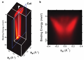
“In solid state physics, the so-called band structure of a material is very important. It describes the relationship between the energy and the momentum of the electrons. The remarkable thing about our surface is that it shows completely different kinds of band structures, depending on the quantum state of the electron”, says Held.

The electron gas in the new material exhibits a multitude of different electronic structures. Some of them could very well be suitable for producing interesting magnetic effects or superconductivity. The promising properties of strontium titanate will now be further investigated. The researchers hope that, by applying external electric fields or by placing additional metal atoms on the surface, the new material could reveal a few more of its secrets.


SOURCE  Vienna University of Technology

By 33rd SquareSubscribe to 33rd Square

Tuesday, November 26, 2013

Nano-SQUID


 Superconctors
Scientists have taken a quantum leap toward understanding the phenomenon known as superconductivity: They have created the world’s smallest SQUID – a device used to measure magnetic fields – which has broken the world record for sensitivity and resolution.


R esearchers have taken a quantum leap toward understanding the phenomenon known as superconductivity: They have created the world’s smallest SQUID – superconducting quantum interference device - used to measure magnetic fields – which has broken the world record for sensitivity and resolution.

Superconductivity is a quantum phenomenon that only occurs when certain materials are cooled to extremely low temperatures. Then, they lose all resistance to the flow of electricity and expel the magnetic fields within them.

Although used in everything from MRI scanners to particle accelerators, scientists still do not fully understand the physics that underlies the behavior of superconductors. Among other things, superconducting materials are found in the very SQUIDs used to measure superconducting properties.

SQUID

Related articles
Nano-SQUIDs are placed on probes to scan and measure the magnetic field at different points on a sample, forming an image of the entire surface – a bit like creating a heat map of a hand by measuring its temperature at individual points on the fingers and palms.

Even very sensitive SQUIDs present geometric challenges when it comes to scanning materials: They need to be as small as possible to attain the highest image resolution, and they need to get as close as possible to the sample to image the tiniest magnetic features. Postdoctoral fellows Drs. Yonathan Anahory and Denis Vasyukov, and PhD student Lior Embon, along with their colleagues in the lab of Prof. Eli Zeldov of the Condensed Matter Physics Department, have risen to the challenge – as reported inNature Nanotechnology – thanks to a unique setup:

They took a hollow quartz tube and pulled it into a very sharp point; then succeeding in fabricating a SQUID encircling the tip measuring a mere 46 nm in diameter – the smallest SQUID to date. They then constructed a scanning microscope around the tip – an achievement that enabled them to obtain magnetic images at distances as small as a few nanometers from the sample. Current SQUID manufacturing methods limit their size and their ability to get very close to a surface. “We have the opposite problem: We have to prevent the probe from ‘crashing’ into the sample,” says Embon.

“While there are SQUIDs with higher sensitivities to uniform magnetic fields, the combination of high sensitivity, proximity of the probe to the sample and its minute dimensions make the overall accuracy of the device record-breaking.” This “nano-SQUID-on-tip” might, in the future, be able to measure the magnetic field from the spin of a single electron – the Holy Grail of magnetic imaging.

According to Zeldov, who is already using the new device to investigate superconductive phenomena in his lab, this invention will hopefully not only lead to a better understanding of superconductivity and vortex flow for the effective application of superconductor technology, but will aid in gaining insights into novel physical phenomena. As a surprising, added bonus, the new SQUID appears to be able to measure many materials other than superconductors.


SOURCE  Weizmann Institute of Science


By 33rd SquareSubscribe to 33rd Square

Tuesday, February 28, 2012

Scientists at IBM Research have achieved major advances in quantum computing device performance that they say may accelerate the realization of a practical, full-scale quantum computer, with quantum states lasting up to 100 microseconds — a 2 to 4 times improvement over previous results. Thes major advances in device performance that may accelerate the realization of a practical, full-scale quantum computer. For specific applications, quantum computing, which exploits the underlying quantum mechanical behavior of matter, has the potential to deliver computational power that is unrivaled by any supercomputer today.
The scientists have established three new records for reducing errors in elementary computations and retaining the integrity of quantum mechanical properties in quantum bits (qubits) — the basic units that carry information within quantum computing.
IBM has employed superconducting qubits, which use established microfabrication techniques developed for silicon technology, providing the potential to one day scale up to and manufacture thousands or millions of qubits.
IBM researchers will be presenting their latest results at the annual American Physical Society meeting taking place February 27-March 2, 2012 in Boston.
The Possibilities of Quantum Computing
The special properties of qubits will allow quantum computers to work on millions of computations at once, while desktop PCs can typically handle minimal simultaneous computations. For example, a single 250-qubit state contains more bits of information than there are atoms in the universe.
These properties will have widespread implications foremost for the field of data encryption where quantum computers could factor very large numbers like those used to decode and encode sensitive information. Other potential applications for quantum computing may include searching databases of unstructured information, performing a range of optimization tasks and solving previously unsolvable mathematical problems.
Quantum states up to 100 microseconds
One of the great challenges for scientists seeking to harness the power of quantum computing is controlling or removing quantum decoherence — the creation of errors in calculations caused by interference from factors such as heat, electromagnetic radiation, and materials defects. To deal with this problem, scientists have been experimenting for years to discover ways of reducing the number of errors and of lengthening the time periods over which the qubits retain their quantum mechanical properties. When this time is sufficiently long, error correction schemes become effective making it possible to perform long and complex calculations.
IBM has recently been experimenting with a unique “three dimensional” superconducting qubit (3D qubit), an approach that was initiated at Yale University. Among the results, the IBM team has used a 3D qubit to extend the amount of time that the qubits retain their quantum states up to 100 microseconds — a 2 to 4 times improvement over previously reported records. This value reaches just past the minimum threshold to enable effective error correction schemes and suggests that scientists can begin to focus on broader engineering aspects for scalability.
In separate experiments, the group at IBM also demonstrated a more traditional “two-dimensional” qubit (2D qubit) device and implemented a two-qubit logic operation — a controlled-NOT (CNOT) operation, which is a fundamental building block of a larger quantum computing system. Their operation showed a 95 percent success rate, enabled in part due to the long coherence time of nearly 10 microseconds. These numbers are on the cusp of effective error correction schemes and greatly facilitate future multi-qubit experiments.
Quantum computing progress
“The superconducting qubit research led by the IBM team has been progressing in a very focused way on the road to a reliable, scalable quantum computer. The device performance that they have now reported brings them nearly to the tipping point; we can now see the building blocks that will be used to prove that error correction can be effective, and that reliable logical qubits can be realized,” observes David DiVincenzo, professor at the Institute of Quantum Information, Aachen University and Forschungszentrum Juelich.
Based on this progress, optimism about superconducting qubits and the possibilities for a future quantum computer are rapidly growing. While most of the work in the field to date has focused on improvements in device performance, efforts in the community now must now include systems integration aspects, such as assessing the classical information processing demands for error correction, I/O issues, feasibility, and costs with scaling.
IBM envisions a practical quantum computing system as including a classical system intimately connected to the quantum computing hardware. Expertise in communications and packaging technology will be essential at and beyond the level presently practiced in the development of today’s most sophisticated digital computers.